‘Magnetoelectric’ material shows promise as memory for electronics
Smartphones and computers wouldn’t be nearly as useful without room for lots of apps, music and videos.
Devices tend to store that information in two ways: through electric fields (think of a flash drive) or through magnetic fields (like a computer’s spinning hard disk). Each method has advantages and disadvantages. However, in the future, our electronics could benefit from the best of each.
“There’s an interesting concept,” says Chang-Beom Eom, the Theodore H. Geballe Professor and Harvey D. Spangler Distinguished Professor of Materials Science and Engineering at the University of Wisconsin–Madison. “Can you cross-couple these two different ways to store information? Could we use an electric field to change the magnetic properties? Then you can have a low-power, multifunctional device. We call this a ‘magnetoelectric’ device.”
In research published recently in the journal Nature Communications, Eom and his collaborators describe not only their unique process for making a high-quality magnetoelectric material, but exactly how and why it works.

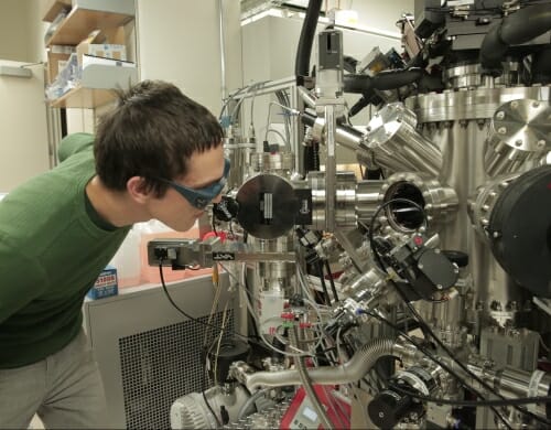
Physics graduate student Julian Irwin checks equipment in the lab of materials science and engineering Professor Chang-Beom Eom, where researchers have produced a material that could exhibit the best qualities of both solid-state and spinning disk digital storage. Photo: Sarah Page
Magnetoelectric materials — which have both magnetic and electrical functionalities, or “orders” — already exist. Switching one functionality induces a change in the other.
“It’s called cross-coupling,” says Eom. “Yet, how they cross-couple is not clearly understood.”
Gaining that understanding, he says, requires studying how the magnetic properties change when an electric field is applied. Up to now, this has been difficult due to the complicated structure of most magnetoelectric materials.
In the past, says Eom, people studied magnetoelectric properties using very “complex” materials, or those that lack uniformity. In his approach, Eom simplified not only the research, but the material itself.
Drawing on his expertise in material growth, he developed a unique process, using atomic “steps,” to guide the growth of a homogenous, single-crystal thin film of bismuth ferrite. Atop that, he added cobalt, which is magnetic; on the bottom, he placed an electrode made of strontium ruthenate.
The bismuth ferrite material was important because it made it much easier for Eom to study the fundamental magnetoelectric cross-coupling.
“We found that in our work, because of our single domain, we could actually see what was going on using multiple probing, or imaging, techniques,” he says. “The mechanism is intrinsic. It’s reproducible — and that means you can make a device without any degradation, in a predictable way.”
To image the changing electric and magnetic properties switching in real time, Eom and his colleagues used the powerful synchrotron light sources at Argonne National Laboratory outside Chicago, and in Switzerland and the United Kingdom.
“When you switch it, the electrical field switches the electric polarization. If it’s ‘downward,’ it switches ‘upward,’” he says. “The coupling to the magnetic layer then changes its properties: a magnetoelectric storage device.”
That change in direction enables researchers to take the next steps needed to add programmable integrated circuits — the building blocks that are the foundation of our electronics — to the material.
While the homogenous material enabled Eom to answer important scientific questions about how magnetoelectric cross-coupling happens, it also could enable manufacturers to improve their electronics.
“Now we can design a much more effective, efficient and low-power device,” he says.
Eom’s team includes both theorists and experimentalists, including UW–Madison physics Professor Mark Rzchowski and collaborators at Diamond Light Source in England, Temple University, the University of Oxford, Argonne National Laboratory, Swiss Light Source, Luxembourg Institute of Science and Technology, and Northern Illinois University.
This work was supported by the Army Research Office (W911NF-10-1-0362 and W911NF-13-1-0486) and the Department of Energy (DE-FG02-03ER46097 and DE-AC02-06CH11357).
Tags: electronics, engineering, materials science, research


