UW getting electron beam lithography system for nanotech research

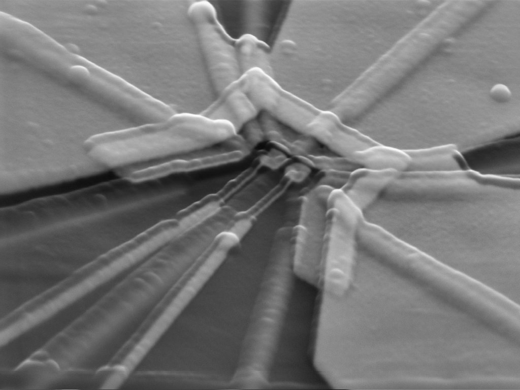
This micrograph shows patterned metal electrodes separated by an insulating layer (transparent in this image), which are used to control the number of electrons in semiconductor quantum devices. It is an example of the type of nanostructure that can be etched with the electron beam lithography system. Trevor Knapp/Eriksson Research Group
Research projects statewide, from electronics to optics and medicine, are set to benefit from a new system coming to UW–Madison that will use electron beam lithography (EBL), a specialized technique for creating extremely fine patterns — in some cases more than 5,000 times narrower than the diameter of a human hair.
The electron beam lithography system, a key instrument required to build devices at the nanometer scale, will give UW researchers and others the ability to work on nanoscale projects with a broad range of possible commercial applications.
The EBL system, valued at about $1.1 million, is expected to be a strong addition to the collaborative environment for researchers within the fields of physics, chemistry, biology, electrical engineering, materials and information technology, and medical research where nanotechnology plays an important role. Mark Eriksson, grant lead on the project and a UW–Madison physics professor, says the system could be used in areas ranging from developing catalyst materials to prototyping computer chips, creating quantum devices and water quality monitoring, and from nanostructured optical metasurfaces to aggressively scaled carbon nanotube field-effect transistors.
The EBL technique consists of scanning a beam of electrons across a surface covered with an electron-sensitive film called a “resist” that can be developed to create a template not unlike a stencil. That pattern can then be transferred into the substrate, either by adding material by deposition or removing material by etching. The electron beam lithography tool can draw devices down to about 10-nanometer resolution on surfaces up to six inches wide. A nanometer is a unit of measurement equal to one billionth of a meter.
“Currently, electron beam lithography in Wisconsin is performed using scanning electron microscopes with conversion systems to enable electron beam writing,” Eriksson explains. “Such converted systems have major limitations, and the new EBL tool will allow for a vast amount of research that was simply inaccessible with past systems.”
The addition of the EBL system is made possible by a $799,996 National Science Foundation Major Research Instrumentation grant. UW–Madison is contributing funds to cover the rest of the instrument purchase, leveraging support from the Wisconsin Alumni Research Foundation, the College of Letters & Science and the College of Engineering. WARF support, totaling $391,000, is provided via the Office of the Vice Chancellor for Research and Graduate Education. The campus is also covering additional costs for renovations and maintenance of the system.
“The new EBL tool will allow for a vast amount of research that was simply inaccessible with past systems.”
Mark Eriksson
The system will become part of the Wisconsin Center for Applied Microelectronics (WCAM), a core research facility managed by the College of Engineering. WCAM provides researchers access to a variety of state-of-the-art nanofabrication tools. Last year, the facility had 170 users from 42 research groups covering six colleges and 19 departments within UW–Madison. WCAM resources have leveraged $65 million in sponsored research to date.
The system’s capability will also be the basis for new modules in existing undergraduate and graduate courses taught in the physics and electrical and computer engineering departments.
“The EBL tool will be a recruitment tool for Graduate Engineering Research Scholars, a unique program that seeks out underrepresented minorities for undergraduate and graduate research positions at UW–Madison,” says Steve Ackerman, associate vice chancellor for physical sciences. “We also will partner with the Interdisciplinary Education Group within the UW–Madison Materials Research Science and Engineering Center to leverage the new system for outreach and education activities, including developing a nanofabrication module for classroom visits at local high schools and creating an online video resource aimed at high schools and the general public to explain nanofabrication techniques and their applications to real-world challenges.”
“The impact of the electron beam lithography tool on research on our campus and beyond will be transformational.”
Marsha Mailick
“This award from NSF validates education and research at UW–Madison, the UW System as a whole, and the entire state of Wisconsin,” Eriksson says, emphasizing the statewide impact of such user facilities. “The co-principal investigators on this award include four faculty from UW–Madison and one from UW-Milwaukee, and planned use by faculty at UW-Platteville, UW-Stevens Point and Marquette University was critical to move this project to completion.”
“The EBL tool adds a powerful new resource to UW–Madison’s research cores toolbox and we congratulate Professor Eriksson on achieving this support from NSF,” says Marsha Mailick, UW–Madison Vice Chancellor for Research and Graduate Education. “The impact of the electron beam lithography tool on research on our campus and beyond will be transformational.”
Tags: nanotechnology, physics, research, science


