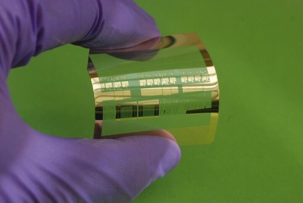
With simple process, engineers fabricate fastest flexible silicon transistor

Using a unique method they developed, a team of UW–Madison engineers has fabricated the world’s fastest silicon-based flexible transistors, shown here on a plastic substrate. Courtesy of Jung-Hun Seo
One secret to creating the world’s fastest silicon-based flexible transistors: a very, very tiny knife.
Working in collaboration with colleagues around the country, University of Wisconsin–Madison engineers have pioneered a unique method that could allow manufacturers to easily and cheaply fabricate high-performance transistors with wireless capabilities on huge rolls of flexible plastic.
The researchers — led by Zhenqiang (Jack) Ma, the Lynn H. Matthias Professor in Engineering and Vilas Distinguished Achievement Professor in electrical and computer engineering, and research scientist Jung-Hun Seo — fabricated a transistor that operates at a record 38 gigahertz, though their simulations show it could be capable of operating at a mind-boggling 110 gigahertz. In computing, that translates to lightning-fast processor speeds.

Zhenqiang (Jack) Ma
It’s also very useful in wireless applications. The transistor can transmit data or transfer power wirelessly, a capability that could unlock advances in a whole host of applications ranging from wearable electronics to sensors.
The team published details of its advance April 20 in the journal Scientific Reports.
The researchers’ nanoscale fabrication method upends conventional lithographic approaches — which use light and chemicals to pattern flexible transistors — overcoming such limitations as light diffraction, imprecision that leads to short circuits of different contacts, and the need to fabricate the circuitry in multiple passes.
Using low-temperature processes, Ma, Seo and their colleagues patterned the circuitry on their flexible transistor — single-crystalline silicon ultimately placed on a polyethylene terephthalate (more commonly known as PET) substrate — drawing on a simple, low-cost process called nanoimprint lithography.
In a method called selective doping, researchers introduce impurities into materials in precise locations to enhance their properties — in this case, electrical conductivity. But sometimes the dopant merges into areas of the material it shouldn’t, causing what is known as the short channel effect. However, the UW–Madison researchers took an unconventional approach: They blanketed their single crystalline silicon with a dopant, rather than selectively doping it.
Then, they added a light-sensitive material, or photoresist layer, and used a technique called electron-beam lithography — which uses a focused beam of electrons to create shapes as narrow as 10 nanometers wide — on the photoresist to create a reusable mold of the nanoscale patterns they desired. They applied the mold to an ultrathin, very flexible silicon membrane to create a photoresist pattern. Then they finished with a dry-etching process — essentially, a nanoscale knife — that cut precise, nanometer-scale trenches in the silicon following the patterns in the mold, and added wide gates, which function as switches, atop the trenches.
The researchers’ nanoscale fabrication method upends conventional lithographic approaches.
With a unique, three-dimensional current-flow pattern, the high performance transistor consumes less energy and operates more efficiently. And because the researchers’ method enables them to slice much narrower trenches than conventional fabrication processes can, it also could enable semiconductor manufacturers to squeeze an even greater number of transistors onto an electronic device.
Ultimately, says Ma, because the mold can be reused, the method could easily scale for use in a technology called roll-to-roll processing (think of a giant, patterned rolling pin moving across sheets of plastic the size of a tabletop), and that would allow semiconductor manufacturers to repeat their pattern and mass-fabricate many devices on a roll of flexible plastic.
“Nanoimprint lithography addresses future applications for flexible electronics,” says Ma, whose work was supported by the Air Force Office of Scientific Research. “We don’t want to make them the way the semiconductor industry does now. Our step, which is most critical for roll-to-roll printing, is ready.”
Additional authors on the paper include Shaoqin (Sarah) Gong of UW–Madison, L. Jay Guo and Tao Ling of the University of Michigan, Weidong Zhou of the University of Texas at Arlington and Alice L. Ma of the University of California, Berkeley.
Tags: computers, engineering, nanotechnology, research


